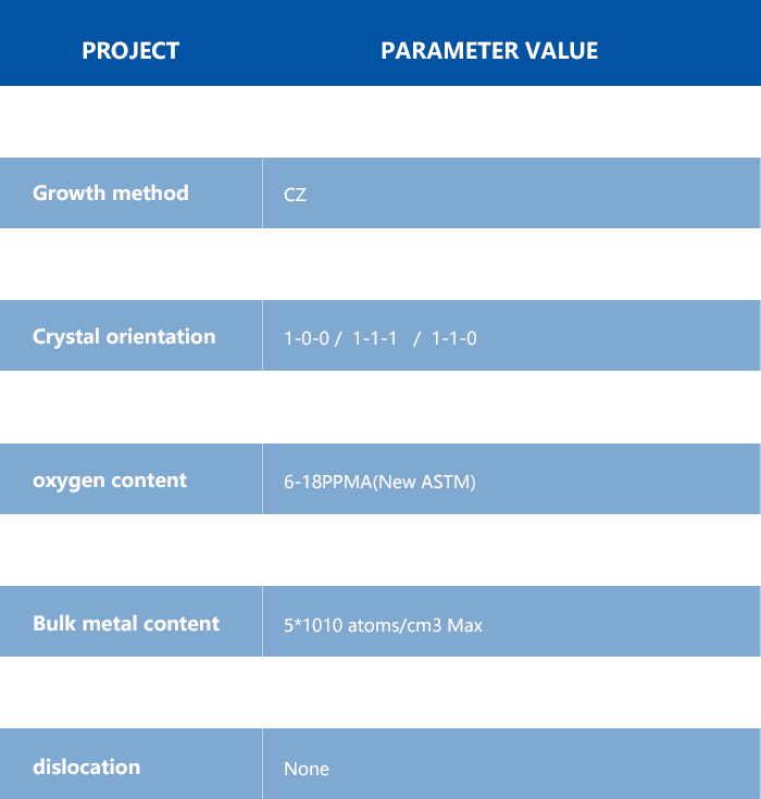
Diameter mm: 100
Model: P, N
Crystal image: < 100 >, < 111 >, < 110 > respectively
With strong processing capacity and process technology support, we can provide products and services to meet customers' needs according to customers' needs or specific specifications.
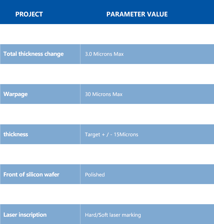
Diameter mm: 100
Model: P, N
Crystal image: < 100 >, < 111 >, < 110 > respectively
With strong processing capacity and process technology support, we can provide products and services to meet customers' needs according to customers' needs or specific specifications.